Could silicon photonics shape future technologies?
A recent article presented a new option in the challenging system bottleneck. This is an issue that has been creating roadblocks to the EMS industry over the last decade.
For years, industry experts are in constant debate on exactly when Moore’s law will cease to apply. Microprocessor architects report that semiconductor advancement has slowed industry-wide since around 2010, below the pace predicted by Moore’s law. However, as of 2018, leading semiconductor manufacturers have developed IC fabrication processes in mass production which are claimed to keep pace with Moore’s law.
Moore’s law is the observation that the number of transistors in a dense integrated circuit (IC) doubles about every two years. Moore’s law is an observation and projection of a historical trend. Rather than a law of physics, it is an empirical relationship linked to gains from experience in production.
Many research facilities and organizations try to find a way to fight the limits that today’s computers have. First memristor and now silicon photonics may lead the way to evolution, bringing a new era with multiple capabilities and options. The processing speeds could get to the next level and AI, IoT, VR, AR can use that extra boost and shape the future. This article was initially published on allaboutcircuits.
As interconnects become an increasingly challenging system bottleneck, some researchers—and even larger corporations like Intel—believe silicon photonics to be a light at the end of the tunnel.
The combined need for device improvement beyond Moore’s Law, along with the diminishing functionality of traditional interconnect schemes, are paving way for the field of silicon photonics. While this field isn’t necessarily new, it is gaining traction. In December 2020, Intel discussed at its annual “Lab Days,” that the company is actively researching silicon photonics “to overcome the limits of electrical I/O by advancing the integration of optical and silicon technologies for future data centers and networks connected by light.”
In this article, we’ll discuss challenges with conventional ICs, the need for silicon photonics, and highlight recent research in which scientists used silicon photonics to create an improved ultrasound sensor.
The Interconnect Bottleneck
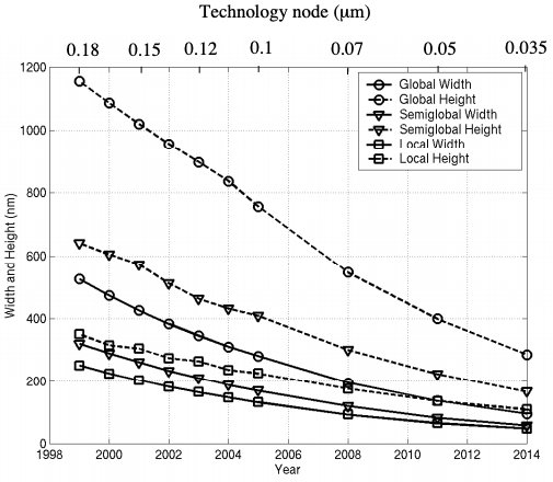
There are two overall trends happening in the IC world currently: devices are getting smaller and chip areas are getting bigger (due to increased integration). The result of these trends is that the interconnect, not the device, is actually becoming one of the biggest bottlenecks in IC design.
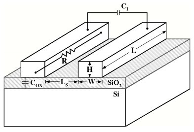
Interconnects, in general, are being forced into smaller geometries with decreased width and thickness while global interconnects, like the clock line, are also becoming longer to accommodate larger chip sizes.
Additionally, increased integration is creating more metal layers that are closer to one another. All of this results in hugely increased interconnect impedances, where parasitic resistances, capacitances, and inductances are becoming more prominent than that of the transistors themselves.
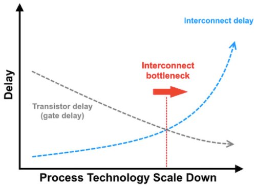
As such, the interconnect is one of the largest contributors to both system delay and power consumption in the form of data movement energy.
Silicon Photonics: A Possible Solution
The solution to these problems, as many believe, is silicon photonics.
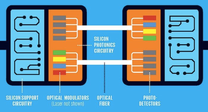
Silicon photonics is a form of IC where photonic integrated circuits are built on silicon. In these circuits, data is transmitted and moved around the chip via light through waveguides as opposed to electrical signals through copper interconnects. The result is a technique that side-steps the increasing concern of the interconnect bottleneck, creating faster ICs without having to scale down the transistor.
The technology has been mostly confined to research to this point, but there is a strong push to eventually bring it to the industry for speed and power-hungry use cases like data centers.
Ultrasound Sensor Based on Silicon Photonics
Proving the value of silicon photonics, a group of researchers from the Interuniversity Microelectronics Center (IMEC) in Europe has developed a silicon photonics-based ultrasound sensor.
Conventional ultrasound sensors use arrays of piezoelectric devices that rely on mechanical resonance at specific ultrasound frequencies. Unfortunately, these techniques are limited by many factors. For instance, the smaller the piezo, the less sensitive it is, hindering its ability to be built into large arrays.
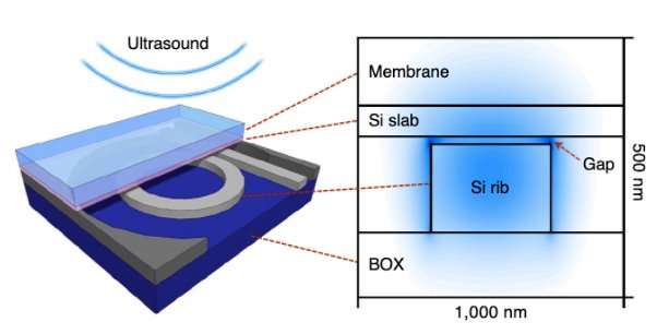
In their article in Nature, the researchers propose a new method that uses a “split-rib” silicon photonic waveguide. The system consists of a main part placed on a movable membrane along with a fixed rib on a substrate. The two are placed in a 15nm-wide gap containing a strong electric field.
When an ultrasound wave distorts the membrane, the electric field will greatly vary the waveguide’s refractive index, which will change the resonance properties of the fixed rib. The researchers were able to use tunable lasers to read out this wavelength, producing an accurate signal.
The Power of Light
The ultrasound sensor proposed in this research is said to have a sensitivity 100 times greater than conventional sensors, showing the power that silicon photonics can offer. As Moore’s Law comes to an end and interconnects become increasingly difficult to work with, a switch to silicon photonics may be just the solution to keep the field advancing.
Our Process
We understand that success begets success and strive for continuous improvement at every level. Applying agile approaches and the latest technological advances, we remain responsive and efficient in our processes, in our manufacturing, and in our service to you.
Ark Electronics is a leading integrated manufacturing solutions provider serving the fastest-growing segments of the global Electronics Manufacturing Services (EMS) market. Recognized as a technology leader, Ark Electronics provides end-to-end manufacturing and engineering solutions, delivering superior quality, support, and delivery services to Original Equipment Manufacturers (OEMs) primarily in the consumer, IoT, industrial and automotive markets. To learn more, please Contact Ark or Request a Quote
Sources:
- https://www.allaboutcircuits.com/news/silicon-photonics-may-remedy-interconnect-bottlenecks-moores-law/
- https://www.intel.com
- https://web.stanford.edu/class/ee311/NOTES/Interconnect%20Scaling.pdf
- http://www2.ece.rochester.edu/users/friedman/papers/ISCAS_05_Optical.pdf
- https://www.researchgate.net
- https://www.synopsys.com
- https://spectrum.ieee.org
- https://www.nature.com
- https://www.bbvaopenmind.com
- https://en.wikipedia.org